
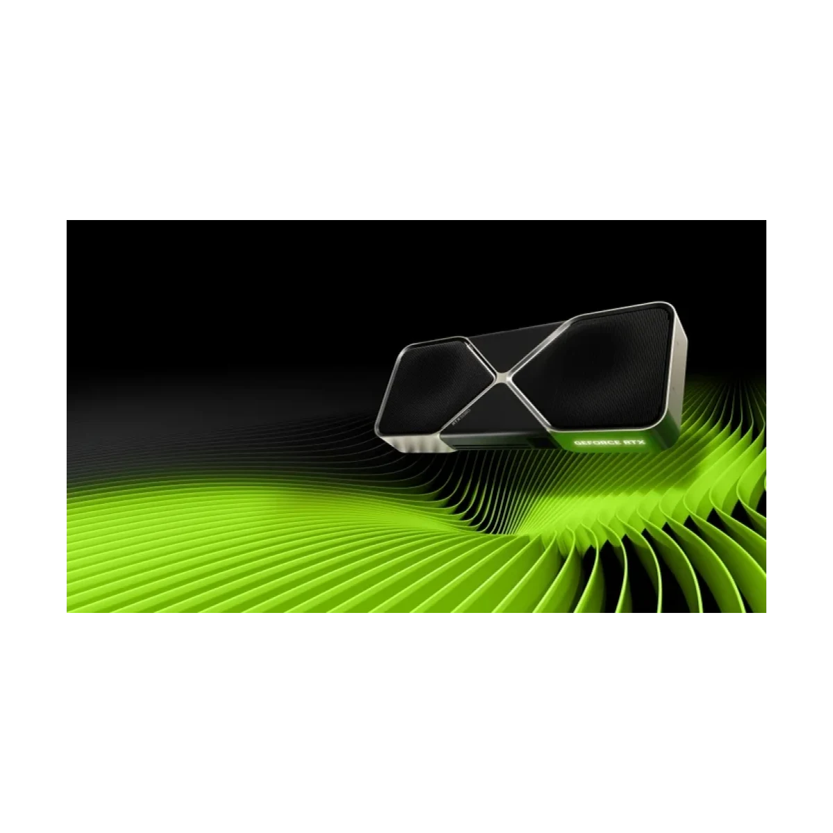
Photo: NVIDIA · Official press image (media use)
GeForce RTX 5080
- Part typeGPU
- Boost clock2.62 GHz
- Video memory16 GB
- Shader units10,752
- Rated power (TDP/TGP)360 W
Official sources Every value below links to the official page it came from.
Zynverse Score · spec-based, not a review · 100% of scored specs known
Calculated only from official specs with fixed, published rules. How the score works
Official launch prices
| Market | Variant | Launch price | Source |
|---|---|---|---|
| GB | starting price | GBP 979 ≈ NGN 1,764,200 | nvidia.com · Jan 2025 |
| US | Founders Edition / starting price | USD 999 ≈ NGN 1,352,080 | nvidianews.nvidia.com · Jan 2025 |
The maker's own launch price per market, as announced. Shop prices change — see “Where to buy” for current offers.
GeForce RTX 5080 overview
NVIDIA GeForce RTX 5080 was announced on 6 January 2025. It is a graphics card with 16 GB of GDDR7 video memory on a 256 bit bus. It has 10,752 shader units and boosts up to 2.62 GHz. Rated power: 360 W (recommended power supply 850 W).
Written from the official specs below — no guesses. Full specs and sources follow.
Full specifications
Launch
| Release date | 30 Jan 2025 Official · nvidianews.nvidia.com · checked 28 Oct 2026 |
|---|---|
| Part type | GPU Official · nvidia.com · checked 28 Oct 2026 |
Core
| Shader units | 10,752 Official · nvidia.com · checked 28 Oct 2026 |
|---|---|
| Base clock | 2.30 GHz Official · nvidia.com · checked 28 Oct 2026 |
| Boost clock | 2.62 GHz Official · nvidia.com · checked 28 Oct 2026 |
| Process | TSMC 4N Official · images.nvidia.com · checked 28 Oct 2026 |
| Architecture | Blackwell Official · nvidia.com · checked 28 Oct 2026 |
Memory
| Video memory | 16 GB Official · nvidia.com · checked 28 Oct 2026 |
|---|---|
| Memory type | GDDR7 Official · nvidia.com · checked 28 Oct 2026 |
| Memory bus | 256 bit Official · nvidia.com · checked 28 Oct 2026 |
Power & connection
| Rated power (TDP/TGP) | 360 W Official · nvidia.com · checked 28 Oct 2026 |
|---|---|
| Recommended PSU | 850 W Official · nvidia.com · checked 28 Oct 2026 |
| Power connector | 3x PCIe 8-pin cables (adapter in box) OR 1x 450 W or greater PCIe Gen 5 cable Official · nvidia.com · checked 28 Oct 2026 |
| Interface | PCI Express Gen 5 Official · nvidia.com · checked 28 Oct 2026 |
Missing a spec? We only add a value once we find it in an official source. Spotted a mistake? Tell us with the source link.
Accessories for the GeForce RTX 5080
Worked out from this phone’s official specs — what fits, what doesn’t, and what to look for.
Power supply
The maker recommends at least a 850 W power supply with a 3x PCIe 8-pin cables (adapter in box) OR 1x 450 W or greater PCIe Gen 5 cable connector.
850 WMotherboard slot
It connects through PCI Express Gen 5; it also works in older PCIe slots at lower bandwidth.
Case
Check the card length and slot width on the board partner's page against your case before buying.
GeForce RTX 5080: common questions
When was the NVIDIA GeForce RTX 5080 announced?
It was announced on 6 January 2025.
What was the launch price of the NVIDIA GeForce RTX 5080?
The official launch price was USD 999 in US (starting price; shop prices change over time).
How much power does the NVIDIA GeForce RTX 5080 use?
Rated power (TDP/TGP): 360 W.
When did the NVIDIA GeForce RTX 5080 go on sale?
Release date: 30 Jan 2025.
What is the part type of the NVIDIA GeForce RTX 5080?
Part type: GPU.
How much VRAM does the NVIDIA GeForce RTX 5080 have?
Video memory: 16 GB.
What power supply does the NVIDIA GeForce RTX 5080 need?
Recommended PSU: 850 W.
What is the shader units of the NVIDIA GeForce RTX 5080?
Shader units: 10,752.
What is the memory type of the NVIDIA GeForce RTX 5080?
Memory type: GDDR7.
Which power connector does the NVIDIA GeForce RTX 5080 use?
Power connector: 3x PCIe 8-pin cables (adapter in box) OR 1x 450 W or greater PCIe Gen 5 cable.
What is the base clock of the NVIDIA GeForce RTX 5080?
Base clock: 2.30 GHz.
What is the memory bus of the NVIDIA GeForce RTX 5080?
Memory bus: 256 bit.
What is the interface of the NVIDIA GeForce RTX 5080?
Interface: PCI Express Gen 5.
What is the boost clock of the NVIDIA GeForce RTX 5080?
Boost clock: 2.62 GHz.
What is the process of the NVIDIA GeForce RTX 5080?
Process: TSMC 4N.
What is the architecture of the NVIDIA GeForce RTX 5080?
Architecture: Blackwell.
Guides & news for GeForce RTX 5080 owners
All guides →
User opinions
No opinions yet. Own this phone? Be the first to share your experience.
Similar pc parts
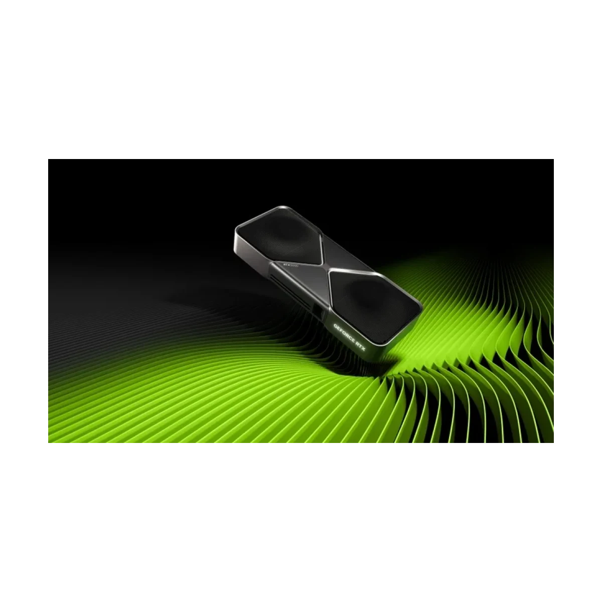 83
GeForce RTX 5090
Announced Jan 2025- GPU
- —
- 2.41 GHz
- 575 W
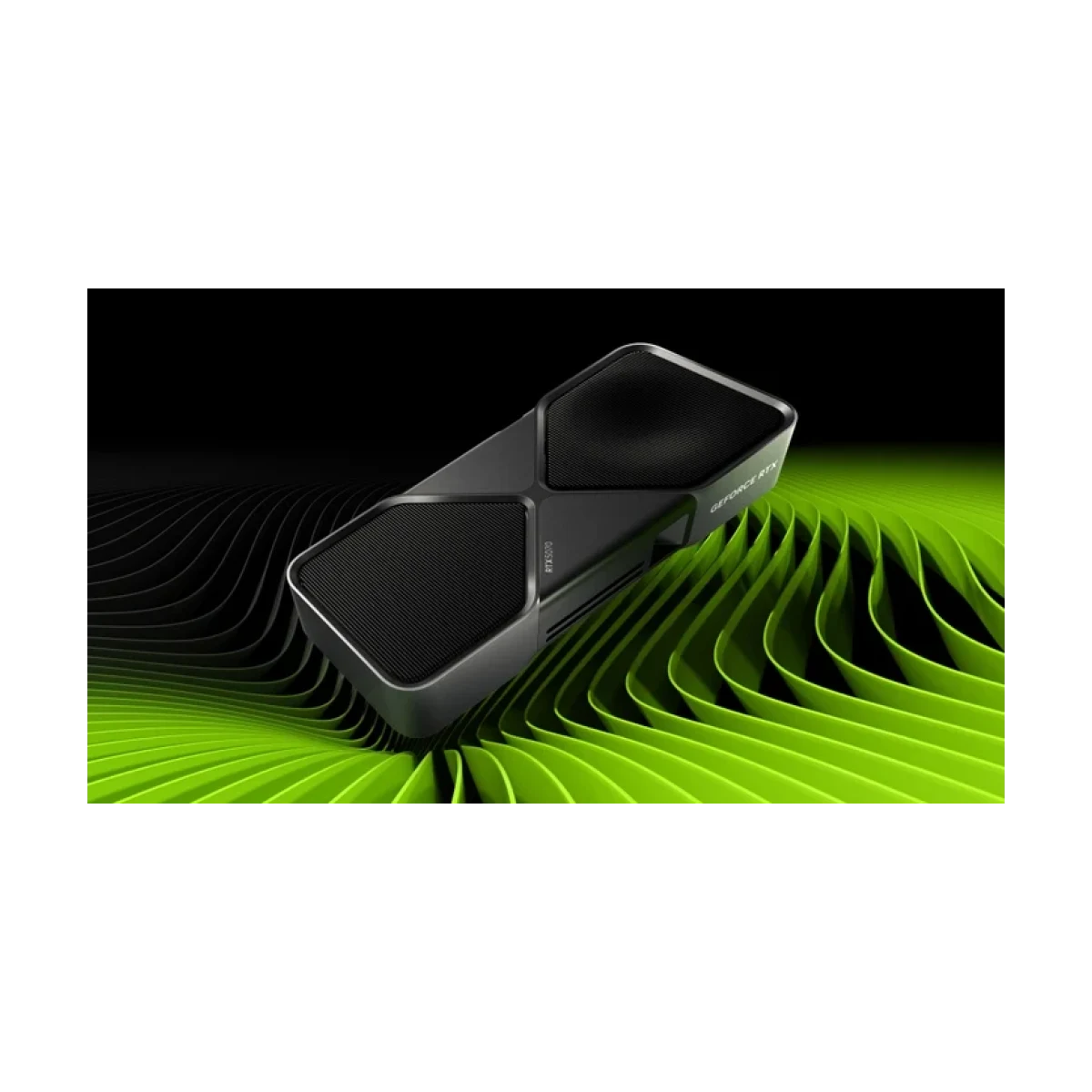 43
GeForce RTX 5070
Announced Jan 2025- GPU
- —
- 2.51 GHz
- 250 W
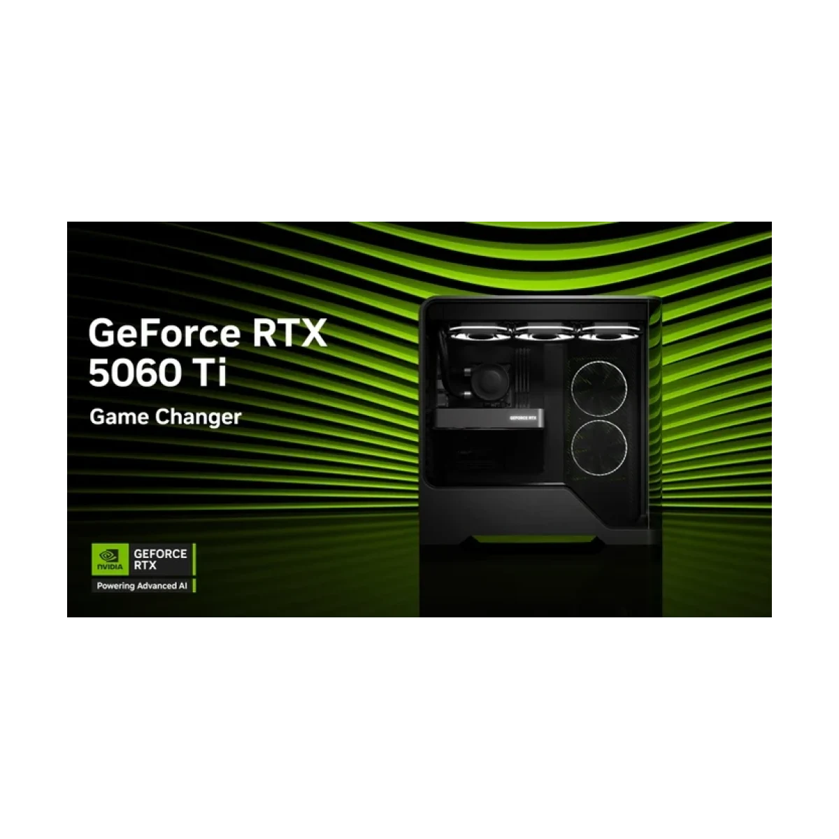 41
GeForce RTX 5060 Ti
Announced Apr 2025- GPU
- —
- 2.57 GHz
- 180 W
Core Ultra 7 270K Plus
Announced Mar 2026- CPU
- 24
- 5.50 GHz
- 125 W